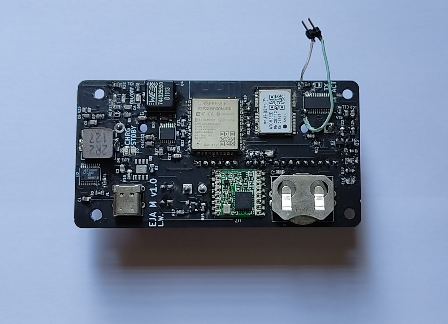
EJA M | 2021 Hackaday Dream Team Challenge
The new EJA M v1.0 is an upgrade/replacement of my older PCB designs: Buoy A v1.0, Buoy B v1.0, and Onboard Gateway v1.0. The design includes the following features:
- USB C Port with Electromagnetic Compatibility (EMC)
- FTDI (FT260S-U) with an Auto Reset Circuit for the ESP32
- ESP32
- GPS Module
- LoRa Transceiver
- Real-time Clock (RTC)
- Connector for a Servo Motor
- 5V 2A Stepup (for the Servo Motor)
- 3.3V Battery Charging Circuit
- 3.3V Battery Charging Circuit
- Connector for a 3 axis accelerometer
- Circuit to measure the battery level
- 3.3V 3A SEPIC Converter
- On-OFF circuit for a Button
- Access to unused pins in the ESP32
This repository contains the Kicad project (including Gerber files).
Planning
Main Objective: EJA M is designed to create a Minimum Viable Product for the EJA Project, it will replace the PCB designs Buoy A, Buoy B and Onboard Gateway. The goal is to maintain the features of the previous designs (some of them are redundant) while achieving the following secondary objectives:
- Reduce the cost. The Bill of Materials of previous designs will be the reference.
- Include battery charging. A feature only present in the previous design Onboard Gateway.
- Reduce the size.
- Measure the battery level.
To achieve these goals, the new design EJA M will replace the development boards that were used in the previous designs with a circuit that contains the main components (ESP32, LoRa, GPS, RTC and power Supply).
The following images present the hardware diagrams for the previous PCB designs Buoy A, Buoy B and Onboard Gateway.
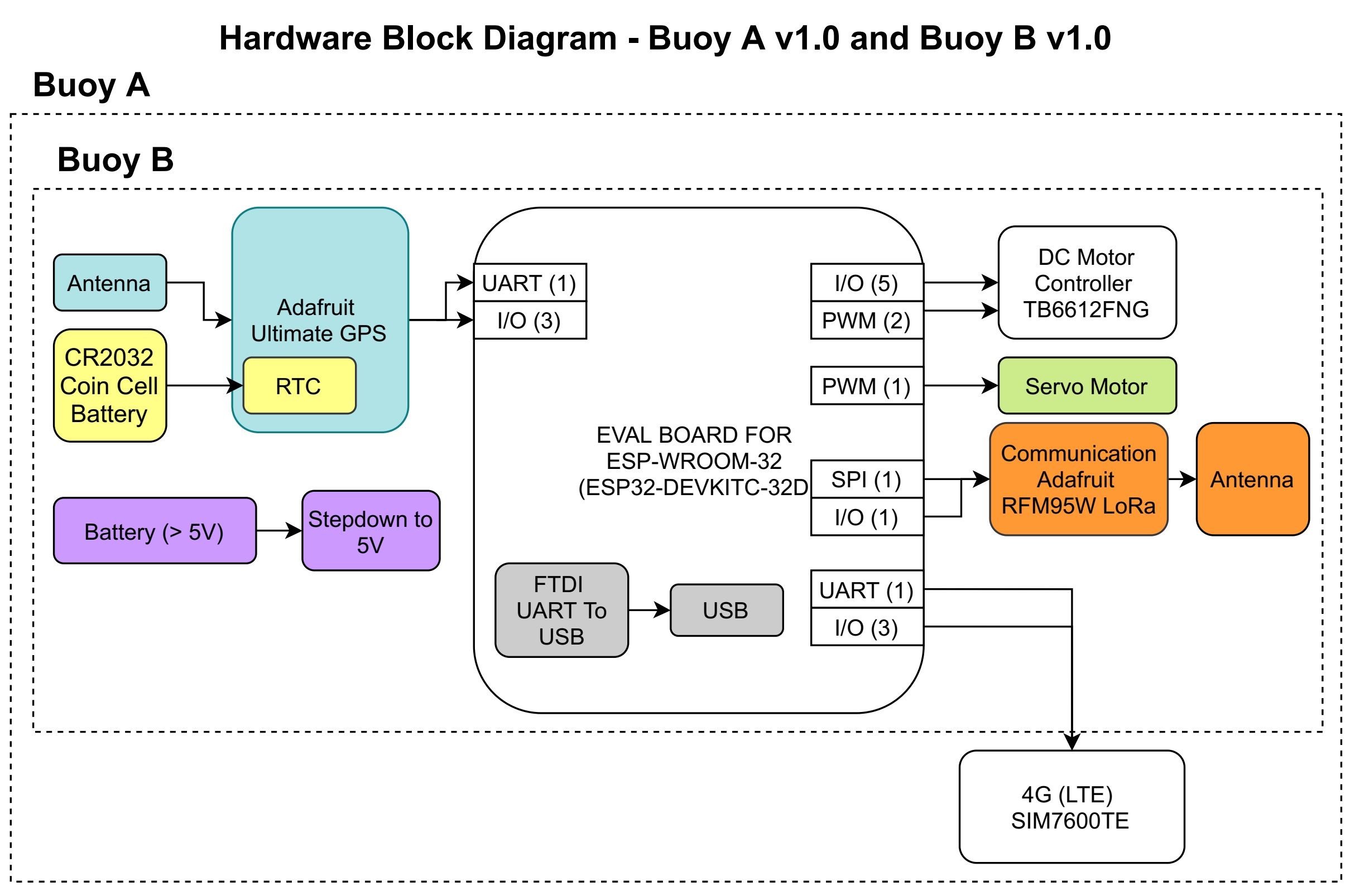
Hardware Block Diagram of the PCB designs Buoy A and Buoy B.
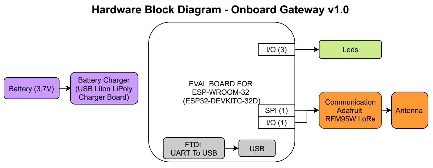
Hardware Block Diagram of the PCB design Onboard Gateway.
Based on the previous images, the hardware diagram of the new design EJA M is proposed. The DC Motor driver (TB6612FNG) and the 4G(LTE) Module, were not included in this design because they are not being used anymore in the project. In the following diagram, the term "Module" refers to a circuit designed by me to adapt the sensor or transceiver to the PCB.
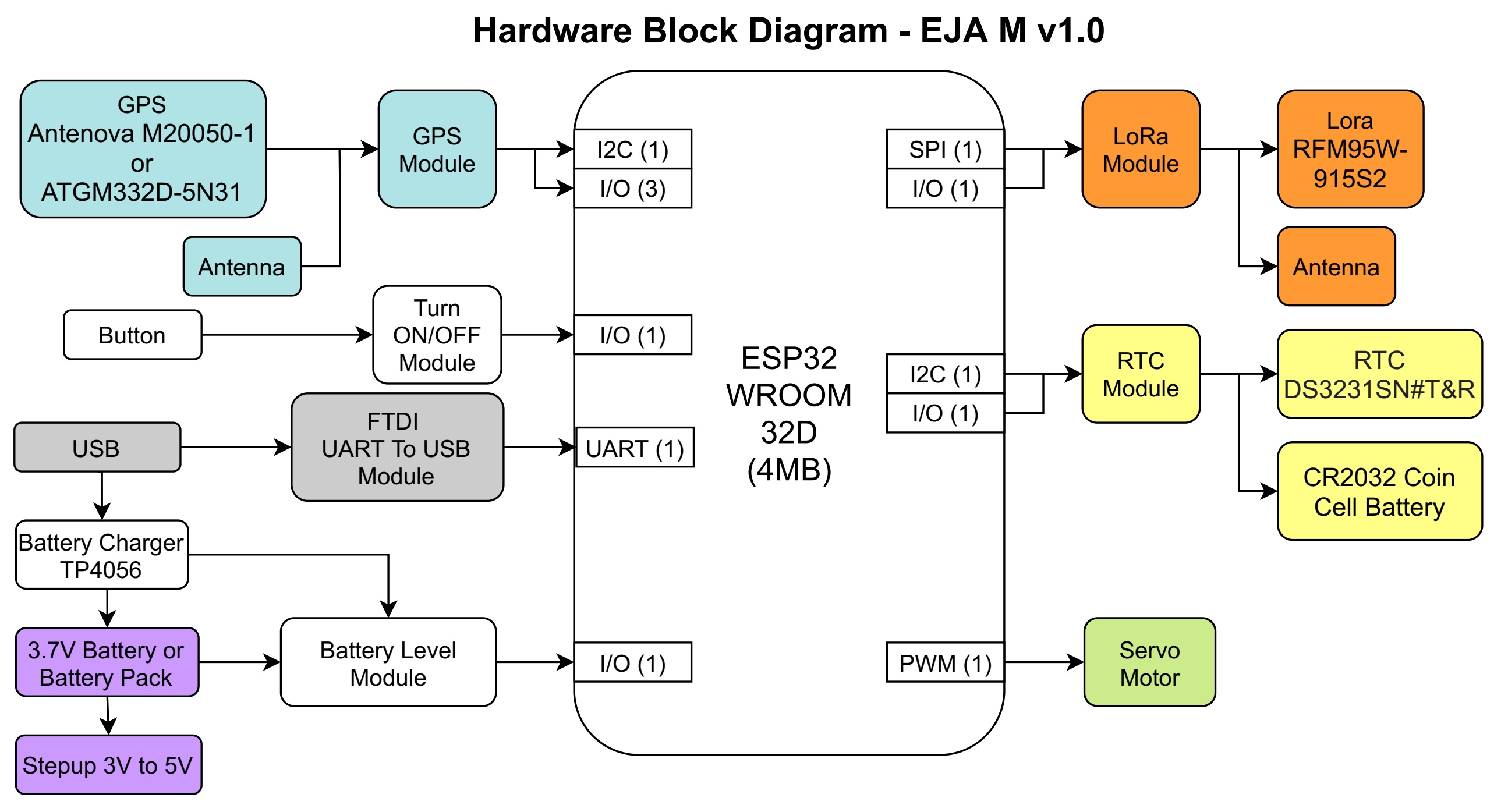
Hardware Block Diagram of the PCB design EJA M.
Hardware Design
USB C Port with Electromagnetic Compatibility EMC
Everything starts with the USB C port, we have chosen this type of USB because it's size and because of the growing trend of using this port to charge and communicate with portable devices.
The design includes Transient Voltage Suppression (TVS) diodes and Ferrite Beads to reduce the Electromagnetic Interference (EMI). These protections for the USB port will add compliance with the EMC regulations and standards from the Federal Communications Commission (FCC) and the European Union.
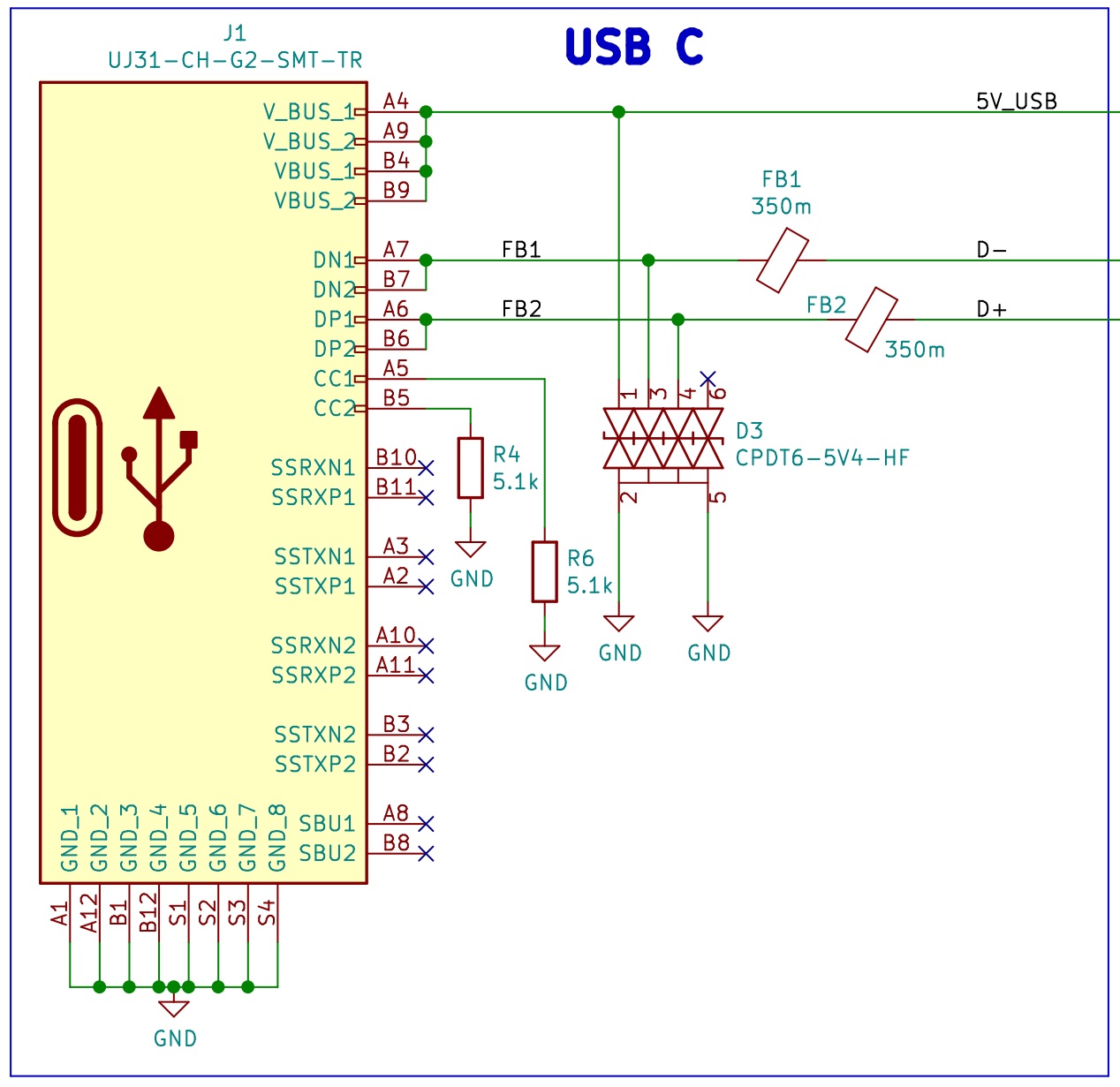
Schematic of EJA M: USB C and EMC protections.
FTDI FT260S
The design includes the FT260S-U, a USB TO UART/I2C FTDI that will be used to program the ESP32.
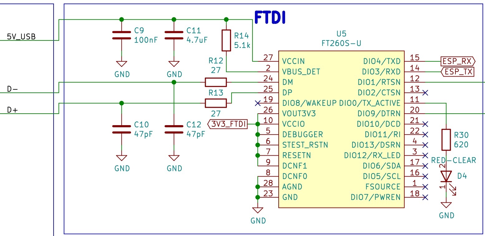
Schematic of EJA M: FTDI circuit using an FT260S-U.
Auto Reset Circuit for the ESP32
The design includes an auto reset circuit that uses RTS and DTR to reset and put in bootloader mode the ESP32. For more information about this circuit, these blogs [1] [2] can be useful.
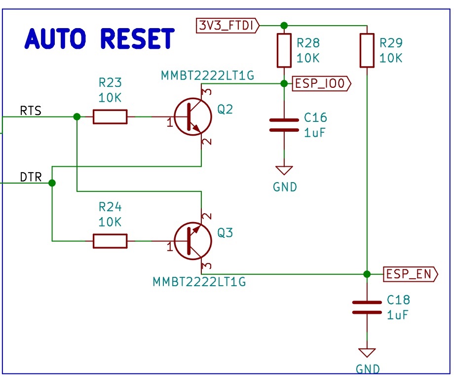
Schematic of EJA M: Auto reset circuit for the ESP32.
ESP32
The main microcontroller in the PCB is the ESP32, the following image shows the signals dedicated to the different pins. The ESP32 is connected to the FTDI, a GPS, a LoRa transceiver, a connector for a servo motor, a real-time clock, a circuit to measure the battery level, a connector for an accelerometer, and a few headers to provide access for the unused peripherals.
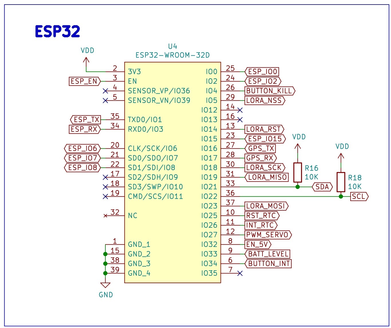
Schematic of EJA M: ESP32.
GPS
The selected GPS is the ATGM332D-5N31, one the modules tested previously in our Development Board for GPS Modules. The schematic is very simple, it has a decoupling capacitors (C2), a U.FL connector for an external antenna (J4) and a Coin Cell Battery Holder (J2).
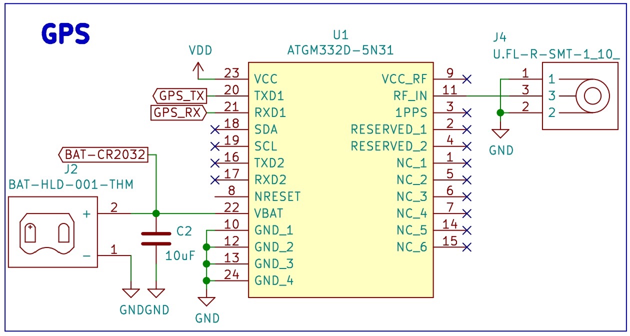
Schematic of EJA M: Circuit for the GPS ATGM332D-5N31.
LoRa
The selected LoRa transceiver is the RFM95W-915S2, the same module tested in our Development Board for LoRa. The schematic contains a U.FL connector for an external antenna (J9).
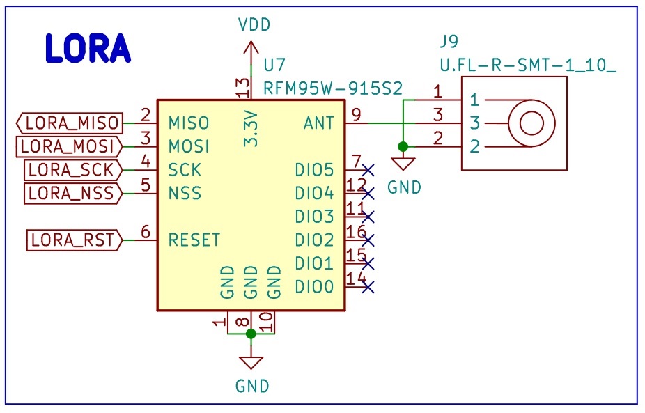
Schematic of EJA M: Circuit for the LoRa transceiver RFM95W-915S2.
Real time Clock RTC
The design includes a dedicated RTC, the DS3231M.
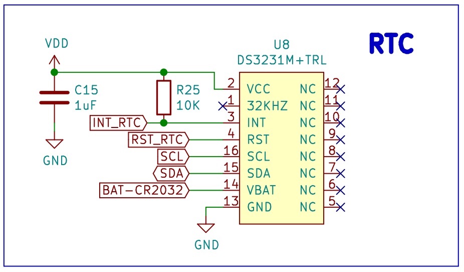
Schematic of EJA M: Circuit for the RTC DS3231M.
Servo Motor Connector
There is a 1x3 header connector for a Servo Motor, the 5V for the servo is provided by a 5V 2A Stepup.
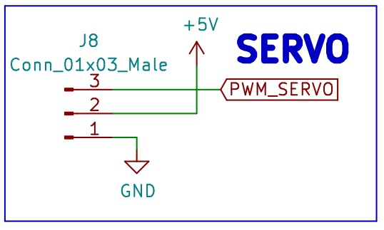
Schematic of EJA M: Connector for the Servo Motor.
5V 2A Stepup
The design includes the TPS61030PWR, a boost converter with a 4A switch current, to provide the 5V for the Servo motor. The schematic contains the components for a 5V 2A output, following the design procedure that starts on the page 13 in the datasheet.
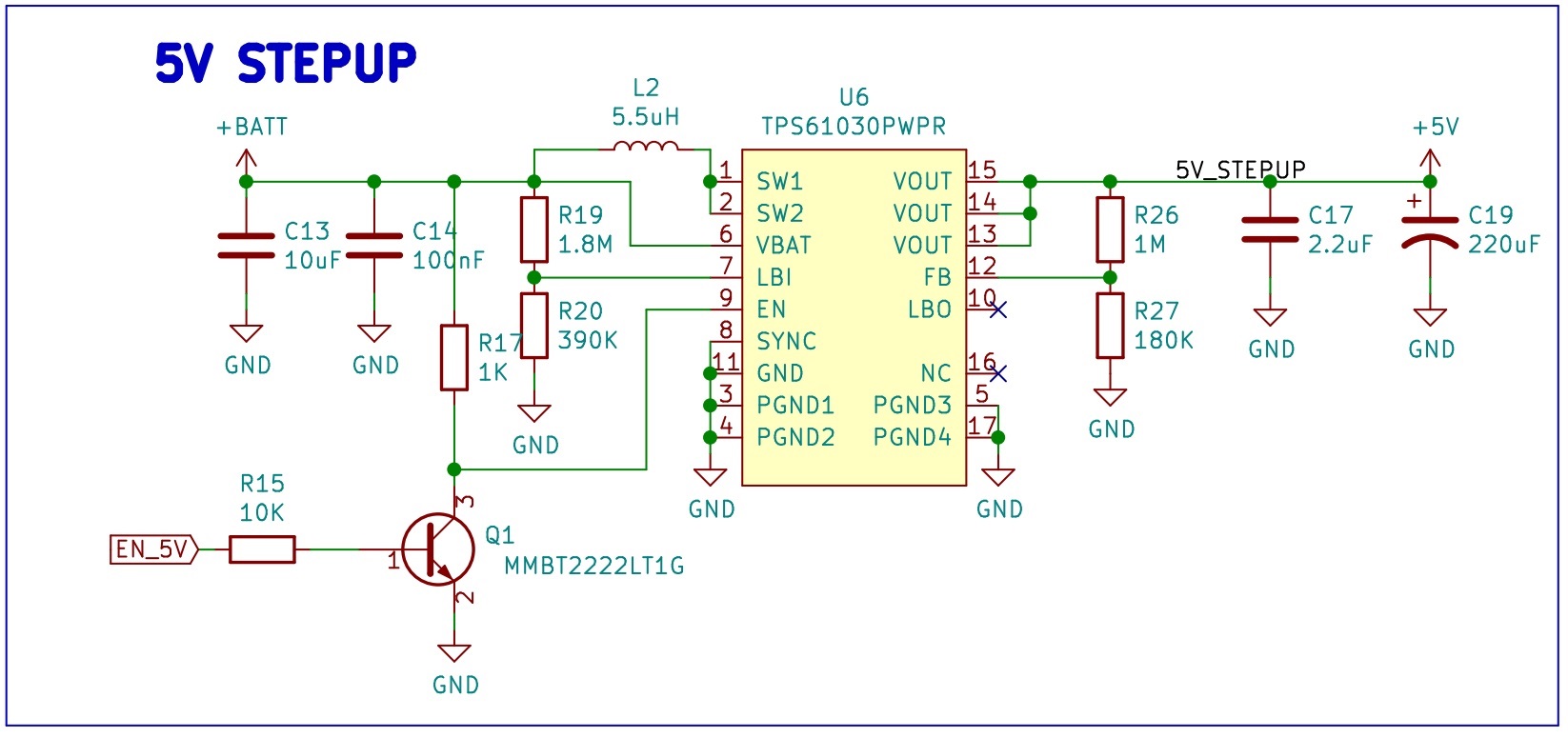
Schematic of EJA M: Circuit for a 5V 2A Stepup using the TPS61030PWR.
Accelerometer Connector
There is a connector for the ADXL343 3 axis accelerometer, a 1x9 header was used even though it only manages the signals VDD, GND, SCL and SDA, in case we want to use more connections for the accelerometer in future versions.
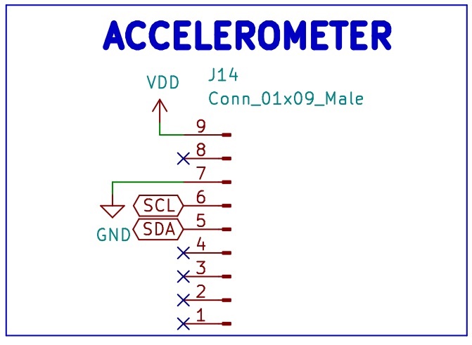
Schematic of EJA M: Connector for the Accelerometer ADXL343.
Battery Charging Circuit
To charge the 3.3V battery the design includes the TP4056, a 1A Standalone Linear Li-lon Battery Charger. The schematic includes a green led to show the user that the battery is charged and a red led to show the user that the battery is charging. There is a Battery Holder for a 18650 battery (J5) and an additional 1x2 header (J7) in case we want to use a different 3.3V battery. There is also a 1x2 header (J3) to use a different type of connection for the charger (instead of the USB C), for example we can connect and test a QI Wireless Charger.
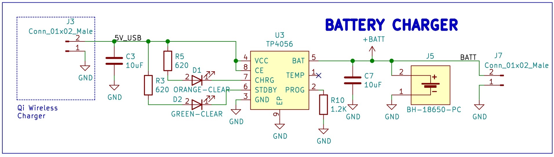
Schematic of EJA M: Battery charging circuit using the TP4056.
Battery Level
The design contains a circuit to measure a battery level, it is a simple resistor divider calculated for a range of 2.7V to 4.2V, the normal range for the 18650 Li-Ion Battery that will be used in the design.
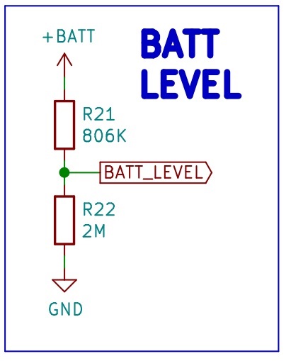
Schematic of EJA M: Circuit designed to measure the battery level.
Those values for the resistor divider give the following range for the ADC:
- Maximum voltage: 4.2V * (2M / (0.806M + 2M)) = 2.99V
- Minimum voltage: 2.7V * (2M / (0.806M + 2M)) = 1.92V
That means that the ADC from the ESP32 will be reading analog values from 1.92V to 2.99V from the battery measurement circuit.
For more information about measuring lithium battery voltage visit the following link.
3V3 3A SEPIC Converter
Since the voltage of the battery can change from 2.7V (discharged) to 4.2V (charged), a SEPIC converter is included to provide a constant 3.3V to the digital circuits regardless of the changes in the input voltage from the battery. The selected SEPIC converter is the LTC3113EFE#TRPBF.
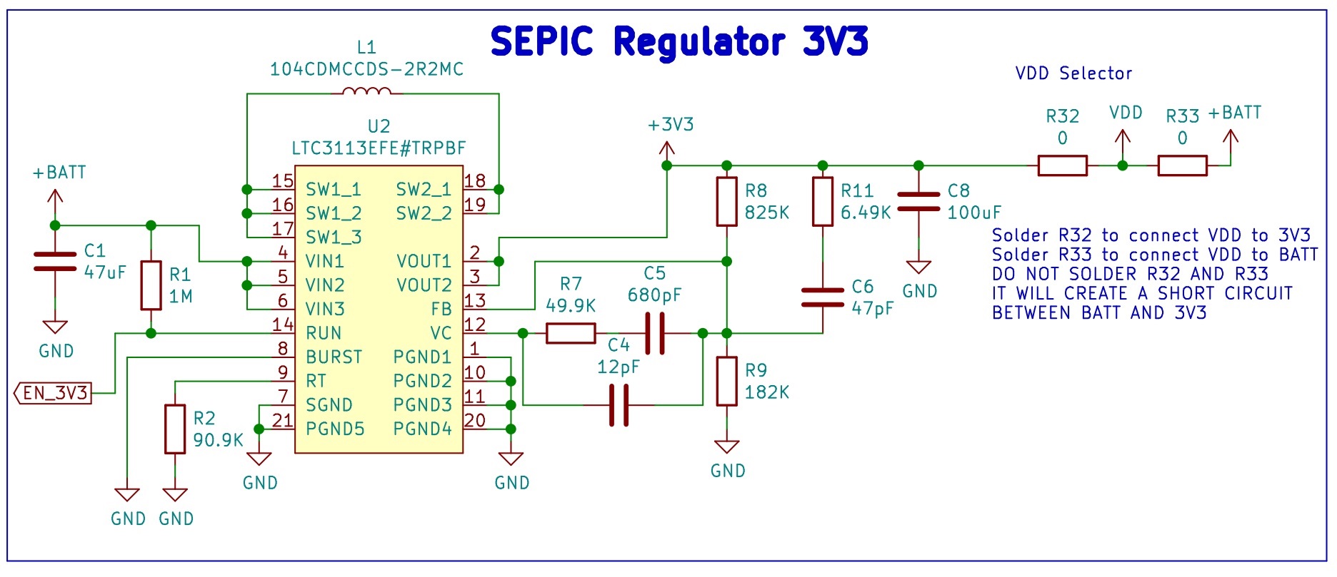
Schematic of EJA M: Design of a 3V3 3A Sepic converter using the LTC3113EFE#TRPBF.
Note: The resistor R32 is a jumper that connects VDD to 3V3. R33 is a jumper that connects VDD to the battery. Do not solder both at the same time, it will create a short circuit between 3.3V from the SEPIC and the voltage from the battery. R32 and R33 are included just in case the SEPIC converter doesn't work and we have to connect the circuit directly to the battery.
Summary: Do not solder R33.
ON-OFF Led
There is Green Led that turns on with the 3.3V from the SEPIC converter, it will notify the user/developer that the device is ON or OFF.
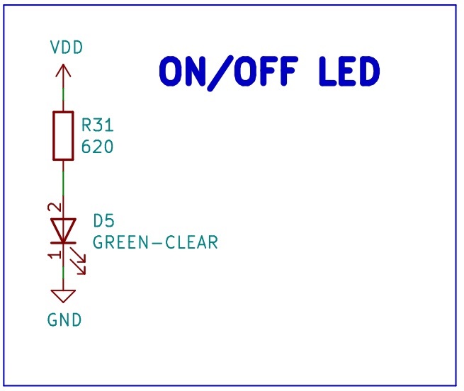
Schematic of EJA M: ON/OFF Indicator.
ON-OFF Button Circuit
The design contains a LTC2954ITS8-1#TRPBF, a pushbutton ON/OFF controller that manages the power supply (enables the 3.3V SEPIC) via a pushbutton interface.
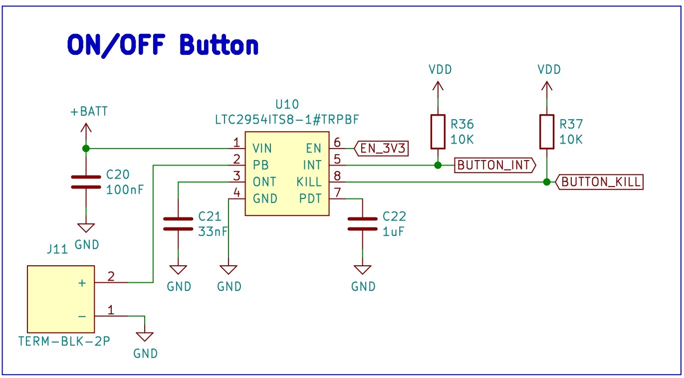
Schematic of EJA M: ON/OFF Circuit using the LTC2954ITS8-1#TRPBF.
Extra Header
The design includes an 1x06 header to provide access for some of the unused pins in the ESP32.
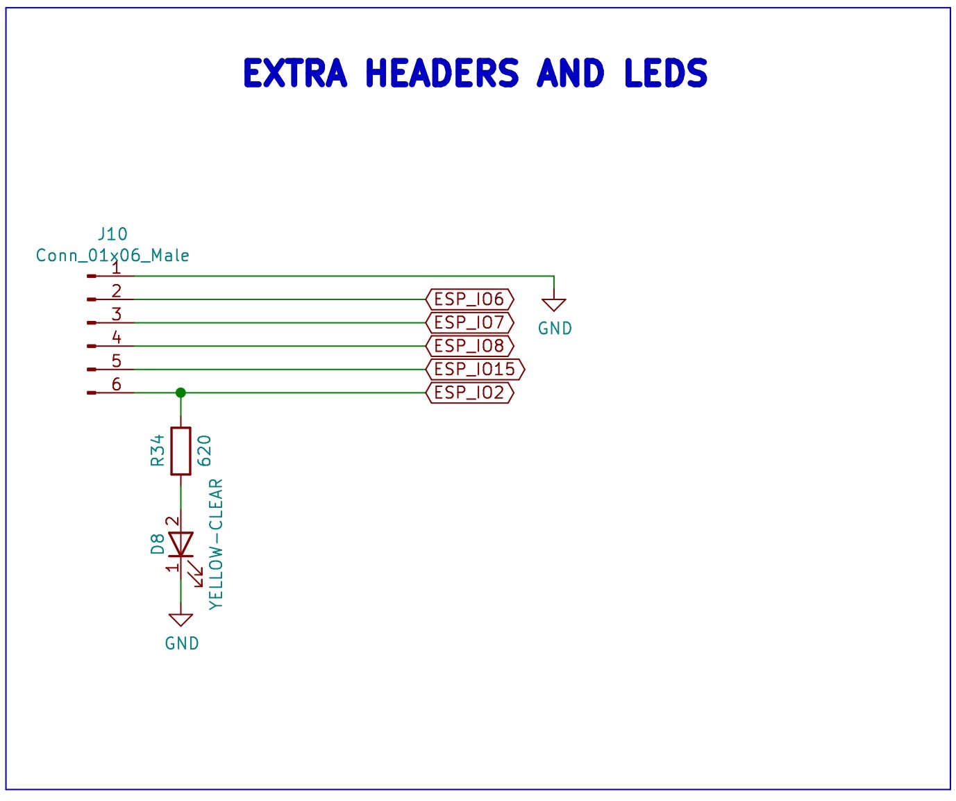
Schematic of EJA M: Header connected to unused I/O ports of the ESP32.
PCB Dimensions and Boundaries
The dimensions of the PCB are dictated by the maximum available space inside the buoy, from the enclosure design we where able to define the size of the PCB: 97.5 mm x 51.2 mm.
In the back layer there is a restricted region, that can't contain any components because the PCB is directly in contact with the enclosure in that region, those are the boundaries of the back layer. Through hole footprints where not be placed in that section, even if the footprint is placed in the front layer.
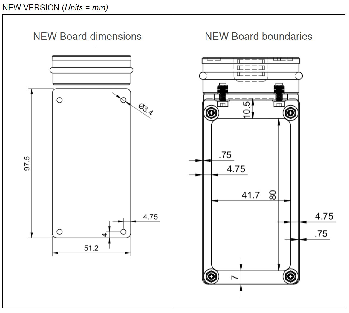
Diagram with the maximum space available for the PCB.
Bill of Materials
PCB Components
Externals Components
For more information about the BOM including prices and different comparisons with my previous designs visit the following link.
PCB
The following images show the front and back layers of the PCB.
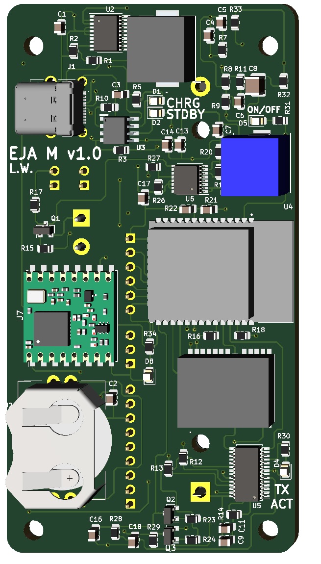
3D Model of the PCB Design.
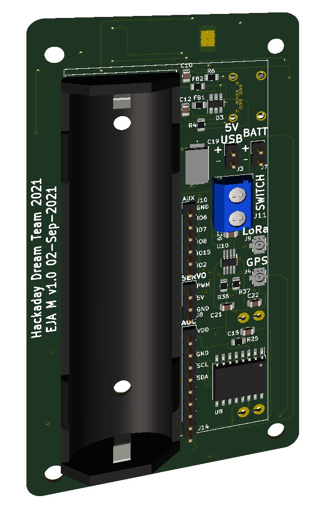
3D Model of the PCB Design.
Posted In:
Embedded Hardware