Buoy A | Hackaday Dream Team 2020
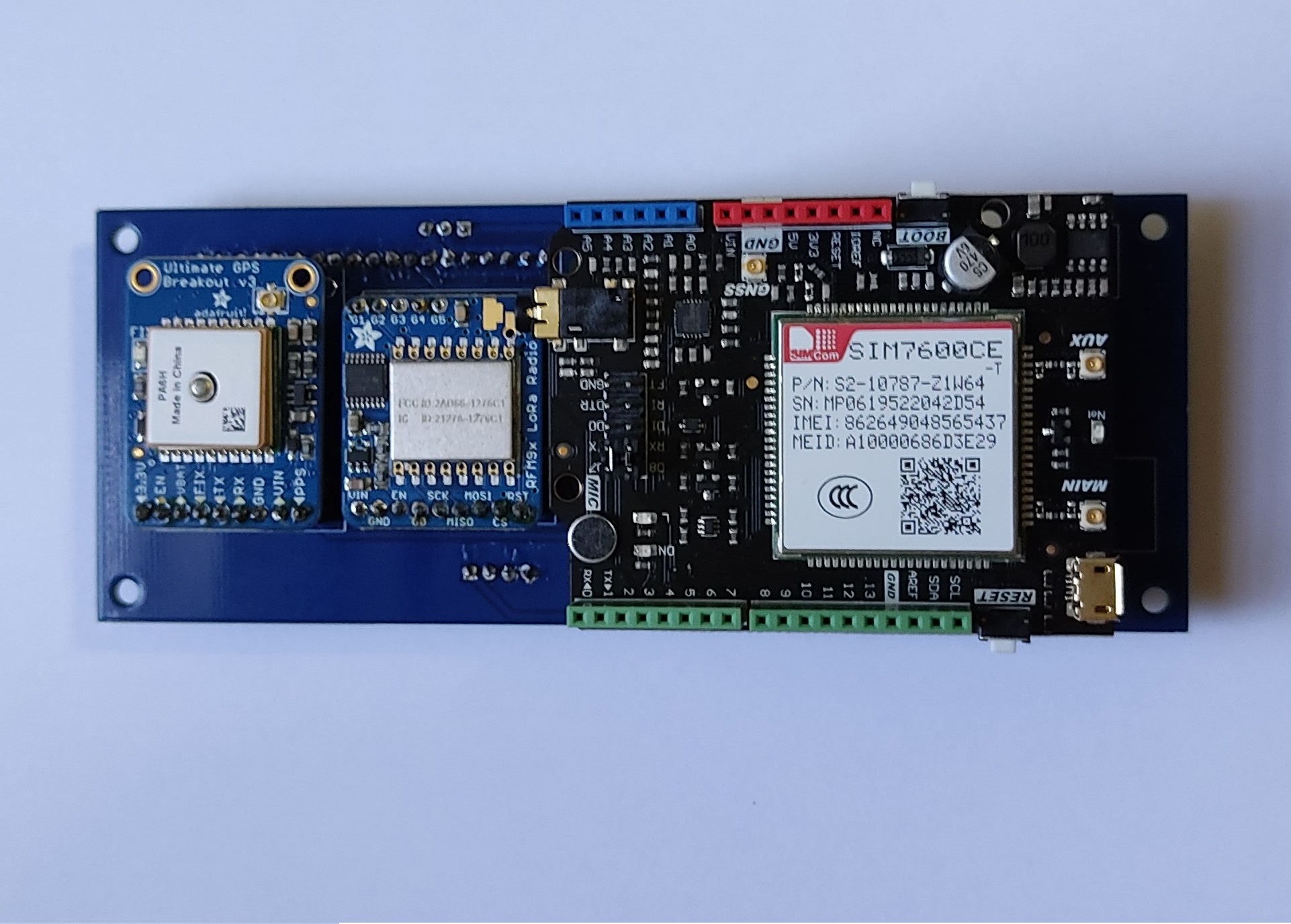
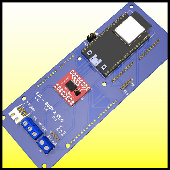
Buoy A V1.0 is a 141.73 mm x 54.86 mm PCB that integrates the 5 main components (ESP32, LoRa, GPS, Motor Driver and GSM/GPRS).
Main Components
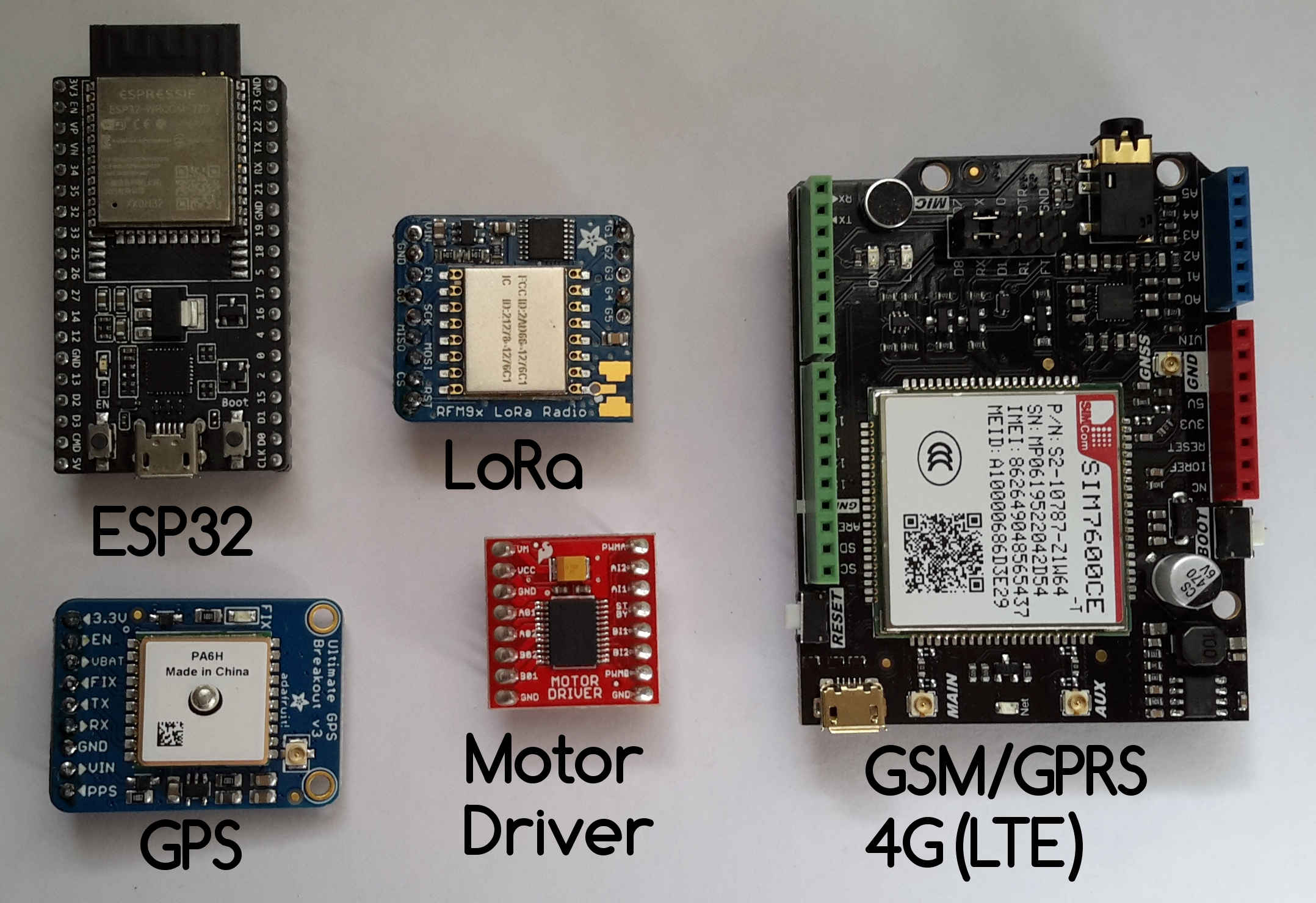
Main components of Buoy A v1.0.
Sources:
- ESP32: ESP32-DEVKITC-32D
- LoRa: RFM95W LoRa Radio
- GPS: Adafruit Ultimate GPS
- Motor Driver: TB6612FNG MOTOR DRIVER BOARD
- 4G(LTE): SIM7600CE-T 4G(LTE) Arduino Shield
Schematic
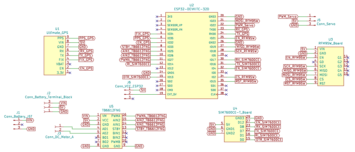
Schematic of Buoy A v1.0.
For more information about the design check the original post in the project's page.
Layout
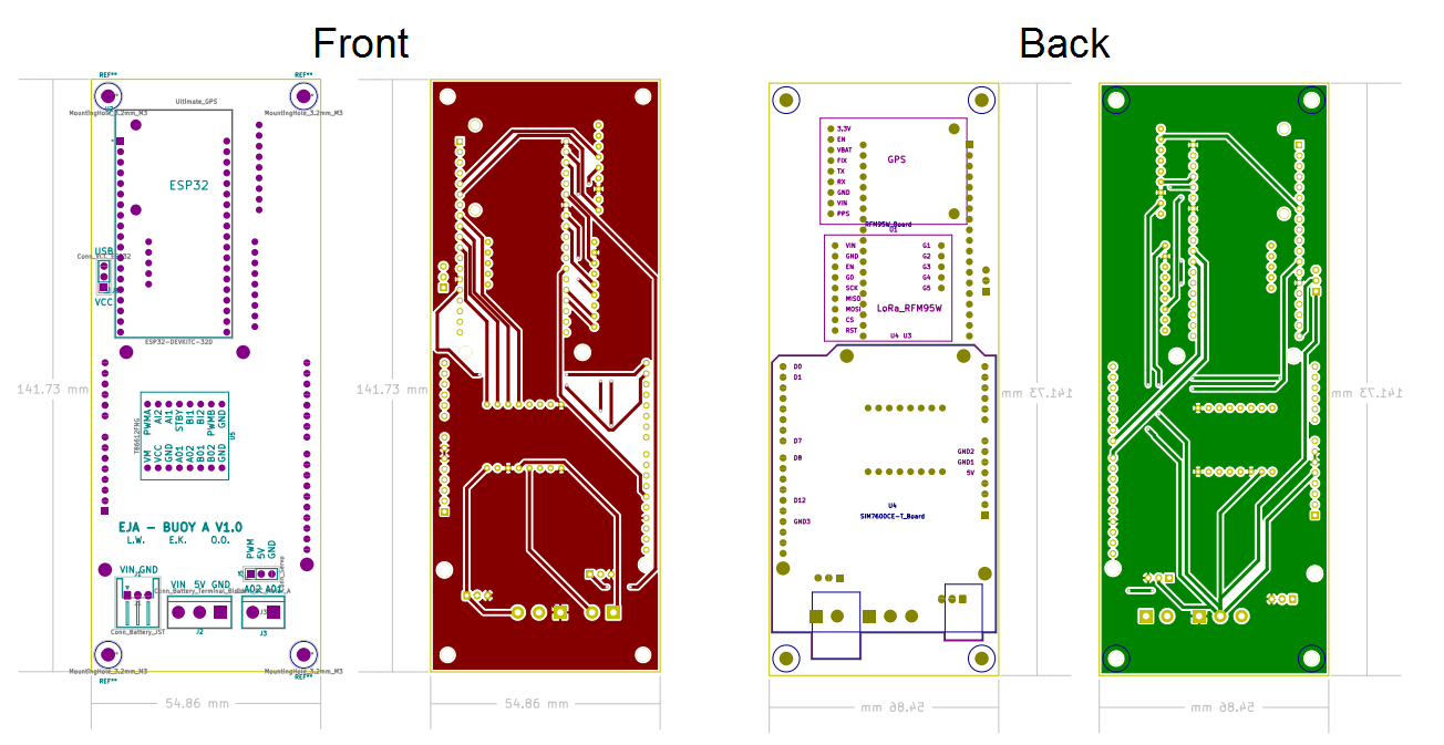
PCB Layout of Buoy A v1.0.
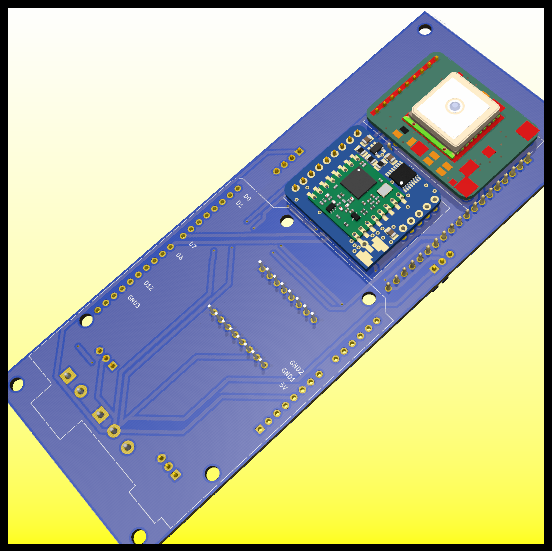
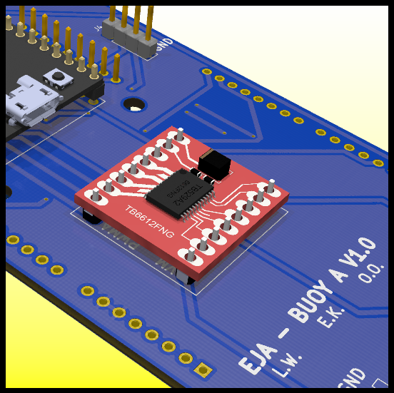
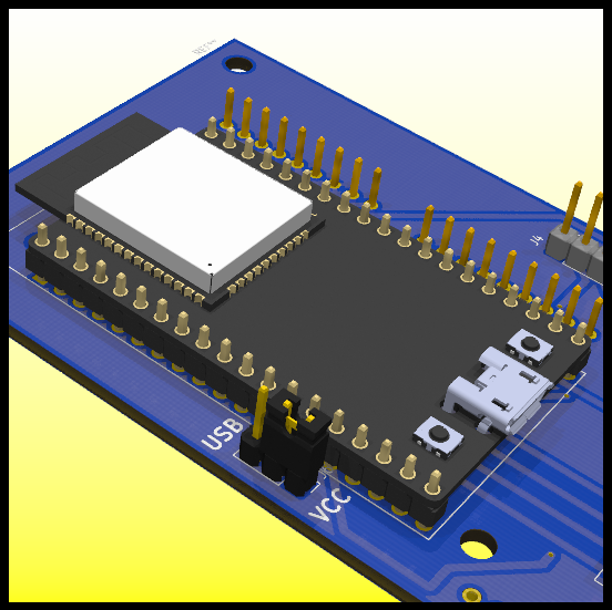
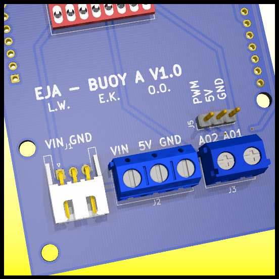
PCB
PCB: Front Layer.
PCB: Back Layer.
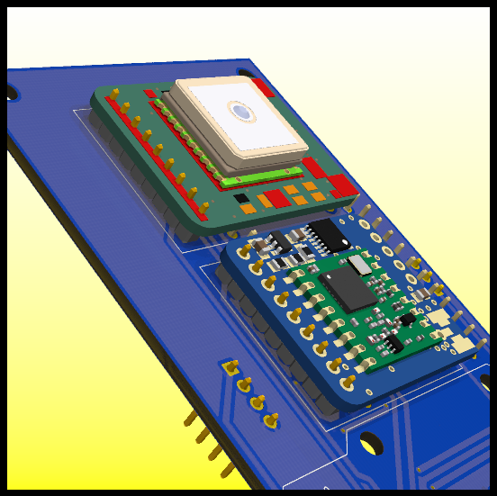
PCB: GPS and LoRa Module.
PCB: Motor Driver.
PCB: ESP32.
PCB: Connectors.
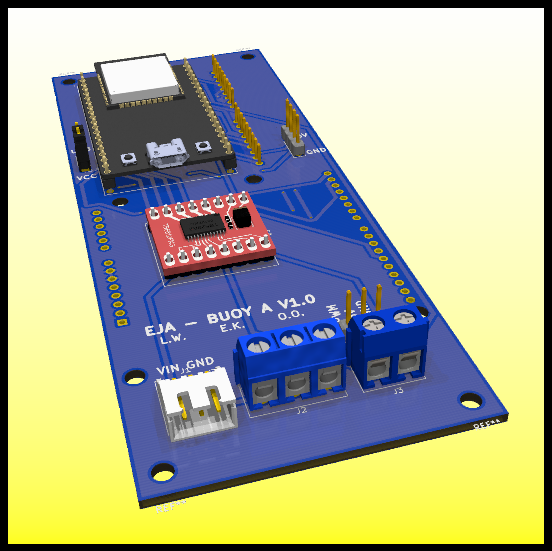
PCB: Front Layer.
Assembly
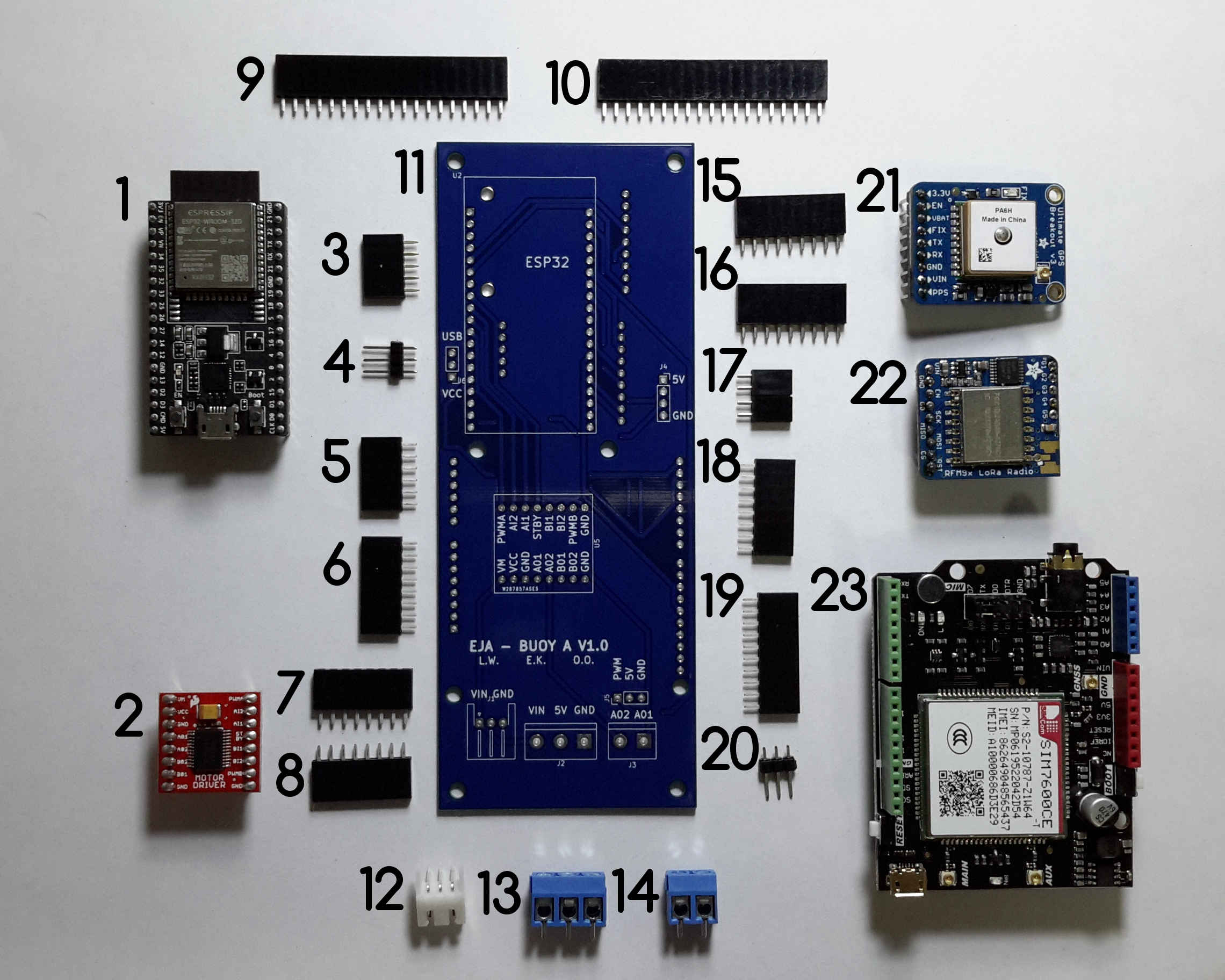
Components of Buoy A v1.0.
Components List:
- ESP32-DEVKITC-32D
- TB6612FNG MOTOR DRIVER BOARD
- CONN HDR 5POS 0.1 GOLD PCB
- CONN HEADER VERT 3POS 2.54MM
- CONN HDR 6POS 0.1 TIN PCB
- CONN HDR 8POS 0.1 TIN PCB
- CONN HDR 8POS 0.1 TIN PCB
- CONN HDR 8POS 0.1 TIN PCB
- CONN HDR 19POS 0.1 TIN PCB
- CONN HDR 19POS 0.1 TIN PCB
- PCB Buoy A V1.0
- CONN HEADER R/A 3POS 2.5MM
- TERM BLK 3P SIDE ENT 5.08MM PCB
- TERM BLK 2P SIDE ENT 5.08MM PCB
- CONN HDR 9POS 0.1 GOLD PCB
- CONN HDR 9POS 0.1 GOLD PCB
- 2 CONN HDR 2POS 0.1 GOLD PCB
- CONN HDR 9POS 0.1 GOLD PCB
- CONN HDR 10POS 0.1 TIN PCB
- CONN HEADER VERT 3POS 2.54MM
- Adafruit Ultimate GPS
- RFM95W LoRa Radio
- SIM7600CE-T 4G(LTE) Arduino Shield
For a detailed Bill of Materials visit the following post.
For a detailed explanation about the soldering and assembly procedure visit the following post.
Wiring Diagrams
The following diagrams present the physical connections of the different boards and components of the Buoy A V1.0:
Power Management
- Battery (5V < Voltage < 15V)
- PCB Board Buoy A V1.0
- Buck Converter
- Switch
- Extra capacitor
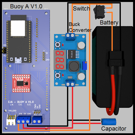
Wiring diagram: Power Management with Buck Converter.
Similar to Buoy B, there is an alternative for the battery management, is possible to provide the required voltages with a boost converter and a 3.7V Battery, like the following example:
- 3.7V 1 Cell Battery
- PCB Board Buoy A V1.0
- Boost Converter
- Micro USB Breakout Board
- Switch
- Extra capacitor
- JST-XH 2 Pos female connector and a JST-XH 2 Pos male connector
- 5V Charger (only used to charge the battery)
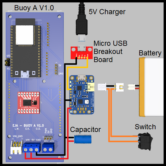
Wiring diagram: Power Management with Boost Converter.
This alternative is valid and possible, but is not ideal for longer working time (compared to the first one). It is important to consider the efficiency of the boost converter. The selected boost converter will have a voltage drop at a current higher than 500mA, that should be taken into consideration.
Motors
The board was designed to handle 2 different types of motors, those are:
- Servo Motor
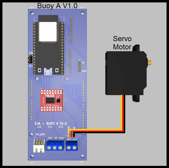
Wiring diagram: Buoy A v1.0 with Servo Motor.
- DC Motor (using the driver TB6612FNG)
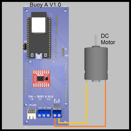
Wiring diagram: Buoy A v1.0 with DC Motor.
For more information about the wiring diagrams and the project visit the following post.
Future Improvements
For more information about the recommended future improvements for the electronic design visit the following post.
Posted In:
Embedded Hardware