Onboard Gateway | Hackaday Dream Team 2020

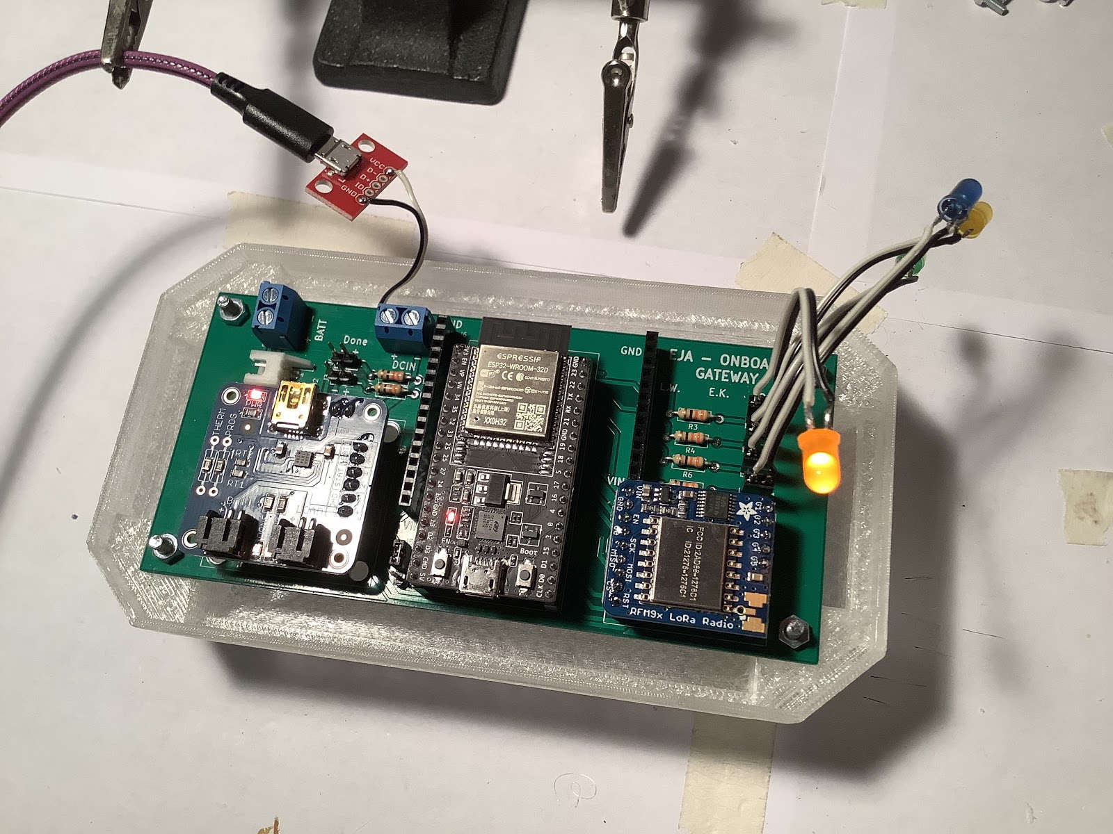
The Onboard Gateway is a 134.11 mm x 62.48 mm PCB that integrates the 3 main components (ESP32, LoRa and USB LiIon/LiPoly charger).
Step 1Define
What It Had to Do
The Onboard Gateway is the topside half of the system: it stays with the operator on the boat and is the link to a deployed buoy. It has no GPS and no motor driver of its own.
- LinkReach a deployed buoy over 915 MHz LoRa (RFM95W) and relay its GPS position and release timer
- InterfaceServe its own web UI over a Wi‑Fi access point, so the operator only needs a phone and a browser
- ControlSet or cancel the buoy's release timer, and show the countdown only once the buoy confirms it
- PowerRun from a single 3.7 V Li‑ion/LiPo cell, charged over USB through the on‑board charger module
- StatusShow LoRa RX, LoRa TX and a connected Wi‑Fi client on LEDs, next to the charger's Charge and Done LEDs
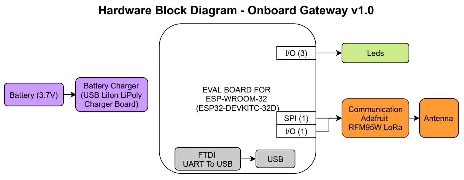
Hardware block diagram of the Onboard Gateway v1.0, from the EJA M planning.
Step 3Build
Main Components
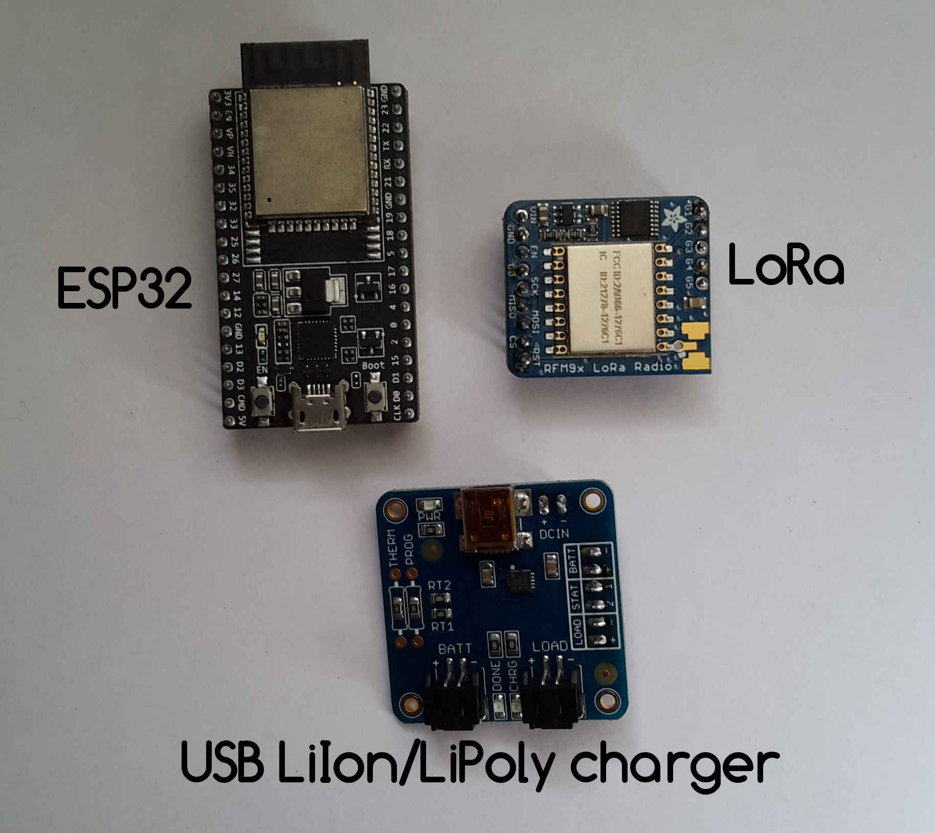
Main components of the Onboard Gateway v1.0.
Sources:
Schematic
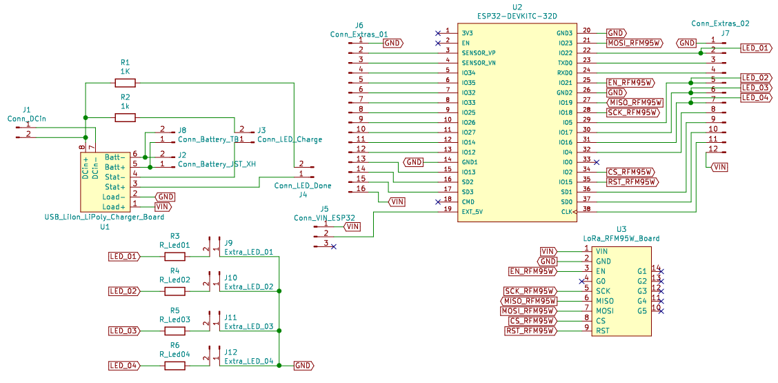
Schematic of the Onboard Gateway v1.0.
For more information about the design check the original post in the project's page.
Layout
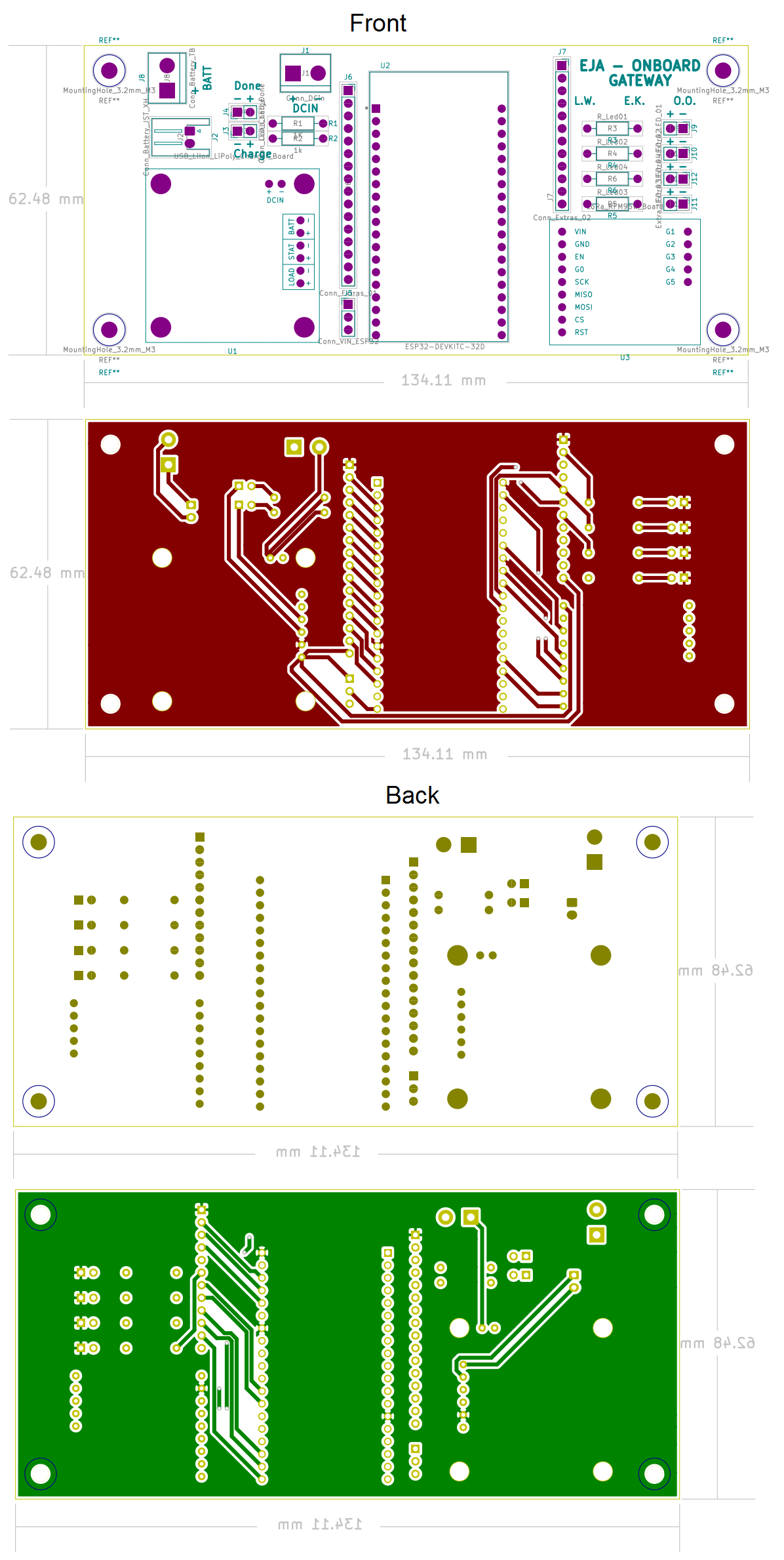
PCB Layout of the Onboard Gateway v1.0.
PCB
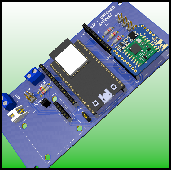
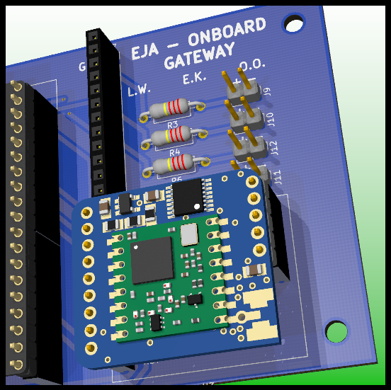
PCB Design.
PCB Design: LoRa Module.
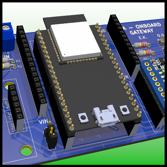
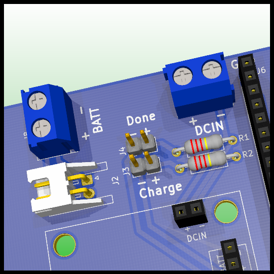
PCB Design: ESP32.
PCB Design: Battery Connection.
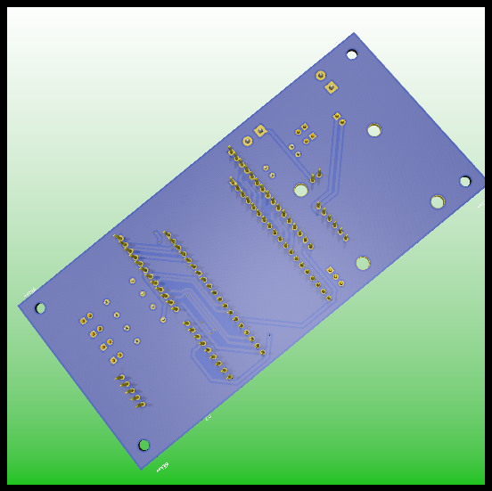
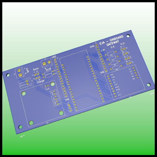
PCB Design: Front and Back.
Assembly
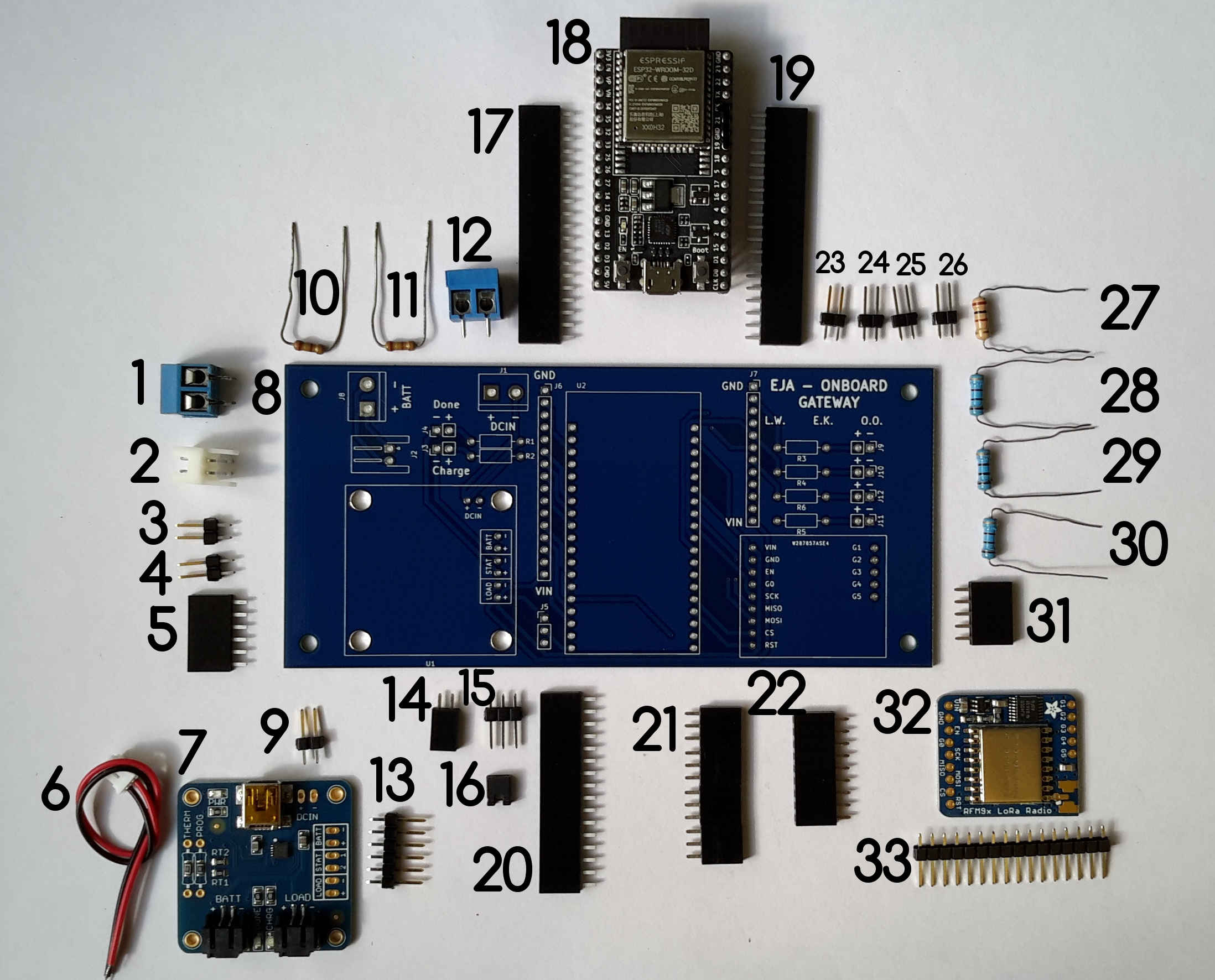
Components of the Onboard Gateway v1.0.
Components List:
- TERM BLK 2P SIDE ENT 5.08MM PCB
- CONN HEADER R/A 2POS 2.5MM
- CONN HEADER VERT 2POS 2.54MM
- CONN HEADER VERT 2POS 2.54MM
- CONN HDR 6POS 0.1 TIN PCB
- 2POS JST cable (included in the USB LiIon/LiPoly charger)
- USB LiIon/LiPoly charger
- PCB Onboard Gateway V1.0
- CONN HEADER VERT 2POS 2.54MM
- RES 249 OHM 1/4W 1% AXIAL
- RES 249 OHM 1/4W 1% AXIAL
- TERM BLK 2P SIDE ENT 5.08MM PCB
- CONN HEADER VERT 6POS 2.54MM
- CONN HDR 2POS 0.1 GOLD PCB
- CONN HEADER VERT 3POS 2.54MM
- CONN JUMPER SHORTING .100" GOLD
- CONN HDR 19POS 0.1 TIN PCB
- ESP32-DEVKITC-32D
- CONN HDR 19POS 0.1 TIN PCB
- CONN HDR 16POS 0.1 TIN PCB
- CONN HDR 12POS 0.1 TIN PCB (I used 2 CONN HDR 6POS 0.1 TIN PCB in the image)
- CONN HDR 9POS 0.1 GOLD PCB
- CONN HEADER VERT 2POS 2.54MM
- CONN HEADER VERT 2POS 2.54MM
- CONN HEADER VERT 2POS 2.54MM
- CONN HEADER VERT 2POS 2.54MM
- RES 100 OHM 3W 5% AXIAL
- RES 100 OHM 3W 5% AXIAL
- RES 100 OHM 3W 5% AXIAL
- RES 100 OHM 3W 5% AXIAL
- CONN HDR 5POS 0.1 GOLD PCB
- RFM95W LoRa Radio
- CONN HEADER VERT 16POS 2.54MM (included in RFM95W LoRa Radio)
For a detailed Bill of Materials visit the following post.
For a detailed explanation about the soldering and assembly procedure visit the following post.
Wiring Diagrams
The following diagram presents the physical connections of the different boards and components of the Onboard Gateway, that includes:
- 3.7V 1 Cell Battery
- Leds (Charge, Done and 4 Miscellaneous)
- PCB Board for the Onboard Gateway V1.0
- 5V Charger (only used to charge the battery)
- Micro USB Breakout Board
- Switch
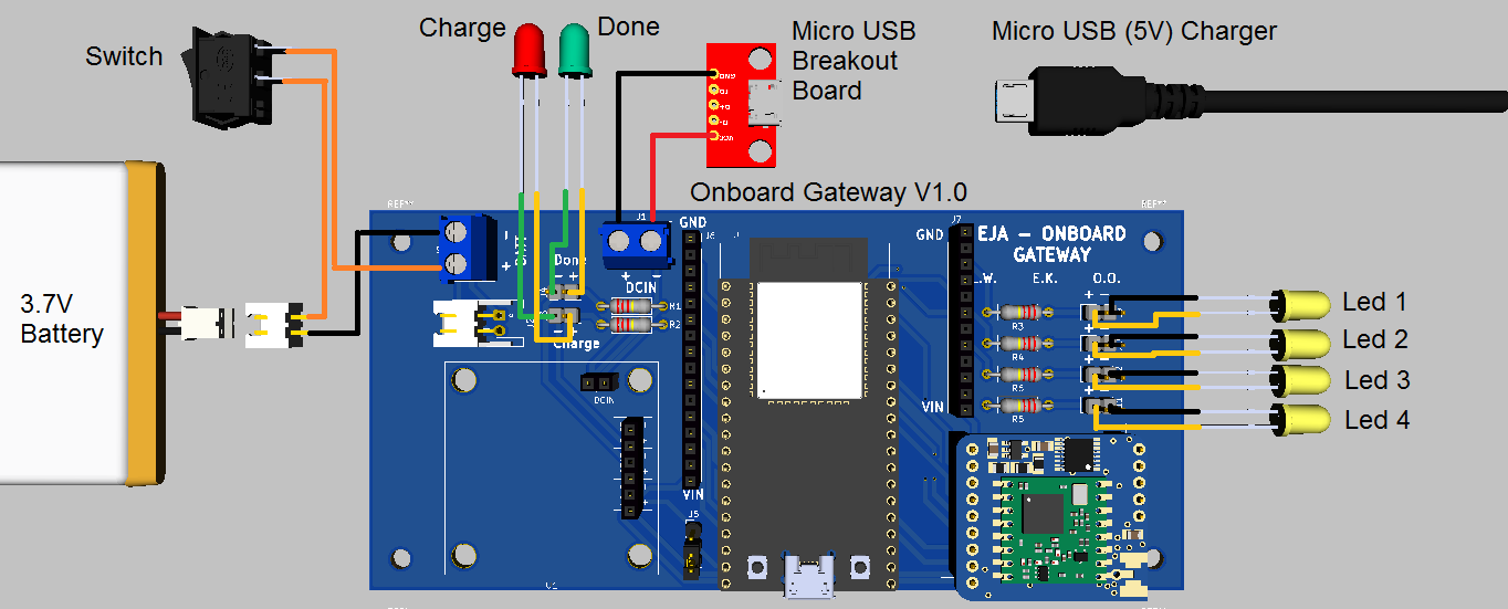
Wiring diagram for the Onboard Gateway v1.0.
Firmware
The Onboard Gateway is the topside unit — it stays with the operator and is a hand‑held LoRa link to a deployed buoy. Its ESP32 firmware mirrors the buoy firmware:
- Captive Wi‑Fi UI —
WiFi.softAP()access pointEJA_Onboard_Gateway, aDNSServermappingwww.onboard_gateway.ejato the ESP32, and an ESPAsyncWebServer serving the UI from SPIFFS with OTA at/update. - LoRa link — RFM95W at 915 MHz (
CSGPIO2,RSTGPIO15,IRQGPIO13). The gateway has no GPS of its own — the position it shows is the buoy's, received over LoRa. Setting a timer sends it to the buoy and only shows the countdown once the buoy confirms; that countdown is an estimate of the one running on the buoy. - Status LEDs — LED1 (GPIO22) LoRa RX, LED2 (GPIO5) LoRa TX, LED3 (GPIO16) Wi‑Fi client connected, LED4 (GPIO17) the web‑controllable test LED.
User Interface
For more information about the GUI visit the following post.
Step 4Test
Bench Bring‑Up
The gateway was run on the bench next to a Buoy B, with a phone connected to the gateway's access point. The gateway has no GPS of its own, so the GPS page on the phone is filled from the buoy's messages over LoRa; in the photo it shows a GPS date and time (16 September 2020, 21:19:56) but 0 satellites and no position fix.
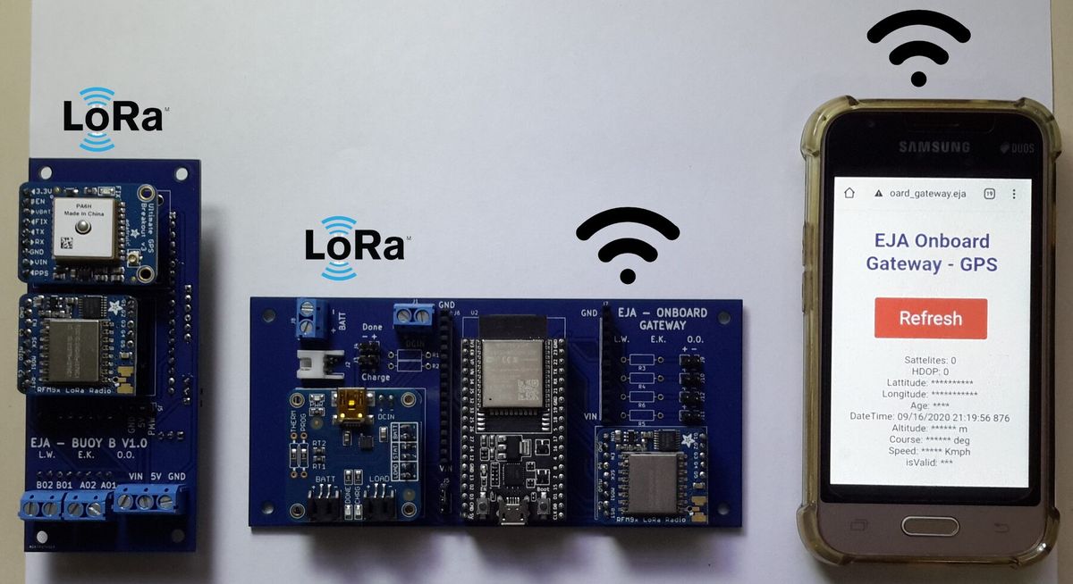
The Onboard Gateway (centre) next to a Buoy B, with the gateway's GPS page open on a phone.
The timer screenshots in the GUI post cover the other direction. After Submit the page reads “Updating timer in Buoy…” while the gateway resends the new end time every second; the firmware only switches to the countdown once the buoy echoes the same end time back over LoRa, and the next screenshot shows that countdown running.
Step 5Refine
Future Improvements
For more information about the recommended future improvements for the electronic design visit the following post.
The Next Board: EJA M
For the project's second prototype, the Onboard Gateway, Buoy A and Buoy B were replaced by a single PCB, EJA M v1.0. Battery charging, which only this board had, became one of the targets in its planning, alongside lower cost (with these boards' bill of materials as the reference), a smaller board and a battery‑level measurement. The plug‑in ESP32‑DevKitC, LoRa breakout and charger board give way to EJA M's own circuits, with a TP4056 linear Li‑ion charger in place of the charger board.
Posted In:
Embedded Hardware